MSc thesis project proposal
Low-temperature epitaxial growth of Ge on Si for CMOS Image Sensors
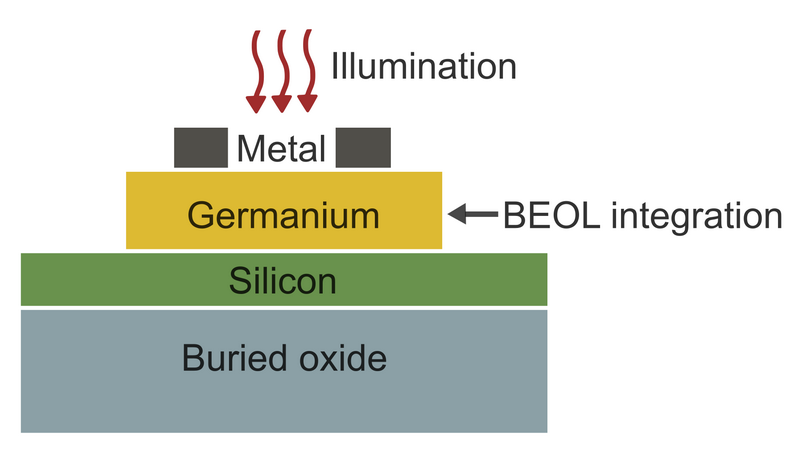
The demand for CMOS image sensors (CIS) covering visible to short-wave infrared is growing in a variety of applications, such as customer imaging, computer vision for self-driving, and surface metrology for defect identification. However, the limited absorption range of silicon (400 nm – 1100 nm) makes it less efficient for detecting wavelengths beyond the visible and near-infrared spectrum. This project aims to overcome silicon's limitations by integrating a germanium layer with silicon CIS using a single-step low-temperature (< 300 °C) process, thus allowing for the incorporation either through post-processing or at the back-end-of-line (BEOL) of a CMOS flow.
You will work under the supervision of two PhD students and will be part of the IS group.
Assignment
In this thesis project, you will:
- Review literature of state-of-the-art low-temperature processes for epitaxial growth of semiconductor layers.
- Define the optimal parameters, e.g., layer thickness, for the experiments.
- Fabricate and optimize your design in EKL.
- Test the device and interpret data results, leveraging electrical testing setups in ECTM.
Requirements
Recommended Background (but not all is required - you can learn in the project!) :
- Semiconductor physics
- Material science
- Cleanroom fabrication
- Excitement about unusual physical phenomena in semiconductors!
Contact
dr. Padmakumar Rao
Electronic Instrumentation Group
Department of Microelectronics
Last modified: 2024-09-03
